Study of origin and control of ferromagnetism in magnetically doped semiconductor: (Ga,Fe)N

Cooperation between groups from Johannes Kepler University (Linz, Austria) and Institute of Physics, PAS, (Warsaw, Poland) belonging to the SPINTRA project has led to a important result for the area of spintronics.
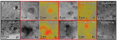
Structural analysis at the nanoscale has shown that the aggregation of Fe ions in (Ga,Fe)N and consequently the magnetic response of the material are affected by the growth rate and doping with shallow impurities. The novel mechanism of nano-self-organisation that has been developed, promises to result in new multi-component semiconductor/magnetic systems, whose characteristics and functionalities can be tuned over a wide range by fabrication parameters, co-doping, and substrate engineering.
For further details about these results read the article: A. Bonanni et al, Phys. Rev. Lett. 101, 135502 (2008) and Phys. Rev. Lett. 100, 03724 (2008)

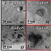
Figure presents various distributions of Fe ions: a diluted random alloy, ferromagnetic FeNx
Fundamental studies of carbon-based nanostructures for spintronics at Poznań

Researchers from Poznan, within the SPINTRA project, have studied spin-polarized transport through carbon nanotubes and graphene.
The results of this research have been published in Phys. Rev. B 78, 035422 (2008).


Conductance and spin-current through a carbon nanotube versus bias and gate voltage (with one paramagnetic and one ferromagnetic contact).

Fabry-Perot-like patterns versus bias and gate voltage for a carbon nanotube
and a graphene nanoribbon
Spintronic nano-devices from Warsaw
 |
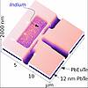
Recently a special attention in spintronic research is devoted to the properties of 3-terminal Y-shaped (or T-shaped) junctions, which act as electron beam-splitters where the injected current separates across two opposite contacts of the ballistic nanodevice. The reason is that such current nanoswitches may be in principle transformed to spin separators or spin entanglers if the injector (bottom part of a Y letter) supplies the supercurrent i.e. when not individual electrons but rather Cooper pairs are branched at the current splitter. For that purpose the construction of the hybrid superconductor-semiconductor (Sc-Sm) devices is necessary. Researchers at the Institute of Physics Polish Academy of Sciences at Warsaw have fabricated a series of 1D hybrid nanostructures containing MBE-grown modulation-doped PbTe quantum wells embedded by Pb$_{0.92}$Eu$_{0.08}$Te:Bi barriers and indium as a superconductor injector (see figure). Low temperature transport measurements of such 3-terminal devices have shown rather unique characteristics of the PbTe/In interface. Quite surprisingly, devices reveal superconducting transition at $\sim 6$K and superconductivity persists in the magnetic fields as high as 7T. Additionally, it has been shown that the interface In/PbTe is extremely transparent (96\%) making it possible to observe pronounced conductance maxima associated with the Andreev reflection. These results make the In/PbTe junction a serious candidate for the development of Y-shaped spin branching devices. Future plans concentrate on examining the Cooper pairs splitting by the application of correlated shot noise spectroscopy analysed with the support from the theory group at the Institute of Molecular Physics Polish Academy of Sciences at Poznañ. High mobility n-type PbTe/PbEuTe quantum wells have been fabricated in Institut f\"ur Halbleiterphysik, Johanes Kepler Universit\"at at Linz. This research is funded by the SPINTRA consortium, lead by Prof. Bogdan Bulka.

